How to Find Model 71861 Register Information
The AXI4 implementationAXI4 is the fourth generation of an interface specification from ARM® commonly used in the semiconductor industry. Xilinx has adopted this standard to create AXI4−compliant plug−and−play IP. Navigator FDK follows the AXI4 standard. For Pentek’s Jade products, the FDK includes the complete IP that is factory−installed in the board. This includes all interface, processing, data formatting, DMA functions, etc. IP designers can modify or replace functions as needed to match application requirements, and will find immediate compatibility with Xilinx IP and third−party IP that uses AXI4. Designers who create their own custom IP using the AXI4 standard will find integration with the Pentek−supplied IP straightforward. in the Jade architecture distributes control registers throughout the block diagrams, which is different from a centralized control register memory map. Because of this, the address information must be navigated in a different way than in the past.
There are several ways to access register information for Model 71861:
- From the Default FPGA Memory Map which includes these categories: Data I/O Interfaces, Data Acquisition, Digital Signal Processing, PCI Express Interfaces, and User Block Address Space.
- From each subsection of the following sections: Data I/O Interfaces, Data Acquisition, Digital Signal Processing DDR4 SDRAM Interface, and PCIe Interfaces
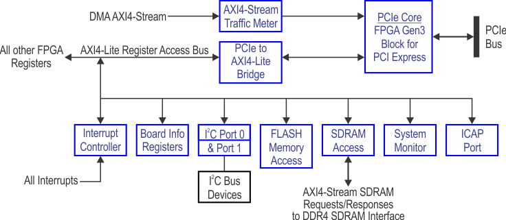
- From the block diagrams below.
Click on any blue block in any of the diagrams below to access register information.
Top−Level Block Diagram

Data I/O Interfaces

Digital Signal Processing

Data Acquisition

PCIe Interfaces

DDR4 SDRAM Interface
