Scenario 2: Customizing the FPGA
If an application requires special processing that only custom IP can provide, the solution is the Navigator FPGA Design Kit (FDK). It was created to work directly with the Xilinx Vivado® Design Suite and creates a seamless environment for developing IP on Pentek products. The Navigator FDK leverages two new features in Vivado to greatly streamline IP development: the AXI4 standard and the IP Integrator.
The AXI4 Standard
AXI4 is the fourth generation of an interface specification from ARM® commonly used in the semiconductor industry. Xilinx has adopted this standard to create AXI4−compliant plug−and−play IP. Navigator FDK follows the AXI4 standard. For Pentek’s Jade products, the FDK includes the complete IP that is factory−installed in the board. This includes all interface, processing, data formatting, DMA functions, etc. IP designers can modify or replace functions as needed to match application requirements, and will find immediate compatibility with Xilinx IP and third−party IP that uses AXI4. Designers who create their own custom IP using the AXI4 standard will find integration with the Pentek−supplied IP straightforward.
The IP Integrator
The FPGA design is edited using Xilinx's IP Integrator, which is a new feature of Vivado. The concept of creating FPGA designs by connecting blocks in a graphical interface, similar to drawing a schematic, is not new, but Xilinx's IP Integrator makes it a practical solution.
To edit a Pentek product design, an FPGA engineer opens the Navigator FDK
design in Vivado, which provides immediate access to the entire board design as
a block diagram. Individual IP cores can be removed, modified, or replaced
with custom IP to meet the application's processing requirements. Because all
blocks have AXI4 interfaces, connections between blocks can simply be
“drawn” with wires or buses and the AXI4 interface handles the “housekeeping” of different bus speeds or widths. (
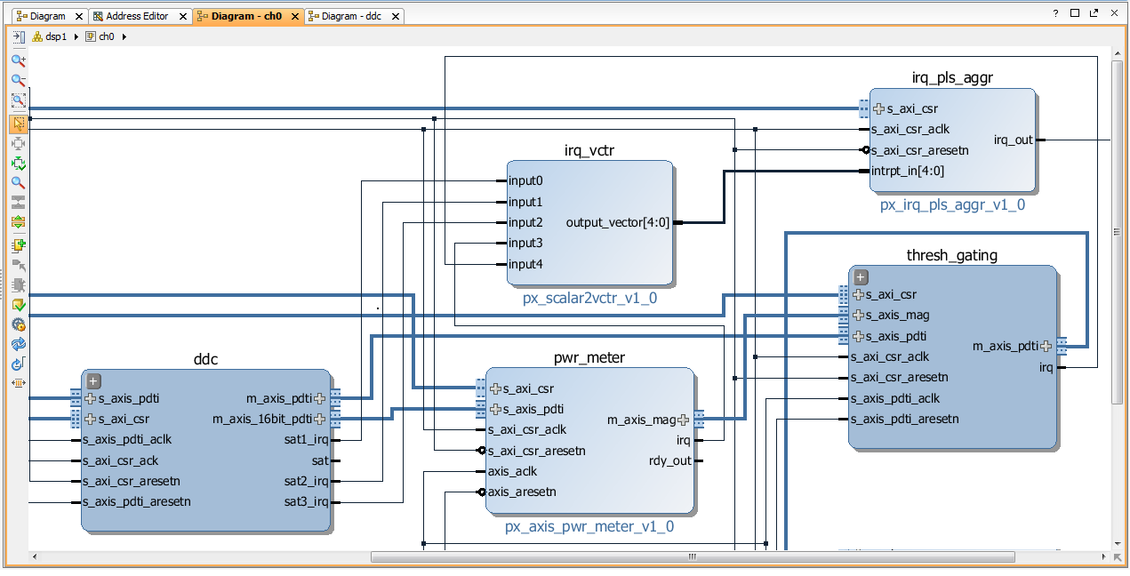
Viewing an FPGA design as a block diagram enables the designer to see the data flow and simplifies the design processes by working at the “interface” and not the “signal” level. If, at any time, a designer needs to work with the VHDL code directly, it is always accessible in a source window. A complete procedure for creating your own IP core is provided in the IP Core Conventions Guide and Example Labs (807.48111 − obtain by contacting sales@pentek.com).
Once a board's function has been modified by changing FPGA IP, it is most likely that changes will need to be made in the software controlling the board to support the new function. While the Navigator Board Support Package (BSP)'s API is ideal for creating applications for the board, it assumes the board functions have not changed from the factory−installed set. So the next step would be to follow the procedure for adding an IP core to the Navigator BSP, which is found in the Navigator BSP User’s Guide.
Details about the API can be found in the Navigator API Reference Guide.