The Model
The block diagram below illustrates the interrupt signal routing on Model
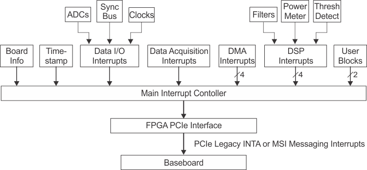
Interrupt events are edge−detected and latched in second−level interrupt flag registers. In addition, the interrupt sources are also routed to dynamic interrupt status registers. The interrupt edges from various sources can be individually enabled by interrupt enable registers and then OR’ed per system module to form sources to the first−level interrupt flag register where the event is latched. Enable bits in the first−level interrupt enable register can individually enable each module’s flag, which are then OR’ed together for a single level interrupt input to the PCIe interface.
Clearing an interrupt in the first−level interrupt flag register will turn off the interrupt. The sources are still latched in the second−level flag register but a new interrupt will not be asserted even if the source is still present until the second−level flag is cleared and the logic subsequently detects a new edge.
Use the Interrupt Controller FPGA IP Core module to control the FPGA PCIe interface interrupt signals.